PCB Cloning & Reverse Engineering
Accurate, secure, and reliable replication of your legacy, obsolete, or undocumented printed circuit boards.
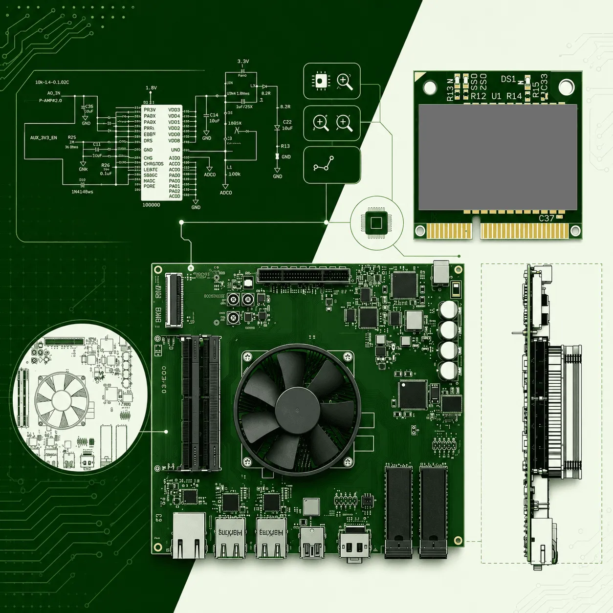
Start Your ProjectWhat is PCB Reverse Engineering?
PCB cloning (or reverse engineering) is the process of analyzing an existing bare or assembled printed circuit board to recreate its original design files, schematics, and Bill of Materials (BOM).
At AEAR, we utilize advanced scanning technology and experienced electronic engineers to extract exact 1:1 Gerber data from physical boards. This service is essential for companies dealing with lost manufacturing files, discontinued components, or the need to upgrade legacy machinery without reinventing the wheel.
- Exact 1:1 Board Replication
- Schematic Diagram Extraction
- Complete BOM Generation
Why Clone a PCB?
Lost Design Files
Original developers or vendors may be unavailable, leaving you with physical boards but no Gerber data to manufacture more. We recover those files.
Obsolete Components
Legacy electronics often use discontinued chips. We reverse engineer the board to update the design for modern, available equivalent components.
System Upgrades
Analyze an existing, working design to understand its architecture, allowing you to add new features or integrate it into a newer system.
Cost Optimization
By recreating the design files, you can freely tender your manufacturing to AEAR or others, breaking free from expensive single-source supplier lock-ins.
Our Reverse Engineering Process
1. Scanning & De-layering
We carefully remove components and scan each layer of the bare board to capture trace paths.
2. Schematic Recreation
Our software and engineers translate the physical scans into precise electrical schematics.
3. Gerber & BOM Generation
We generate manufacturing-ready Gerber files and compile a modern Bill of Materials.
4. Prototyping & Test
We fabricate and assemble a prototype to guarantee the clone matches original functionality.
Frequently Asked Questions
Cloning Specifications
We have the technology to clone highly complex boards, including:
- Up to 32 Layer Boards
- Blind & Buried Vias
- Rigid, Flex, and Rigid-Flex
- High-Frequency & RF Boards
- BGA & Fine Pitch Components
- Complete Encrypted IC Decoding
Need a Board Cloned?
Send us photos of the front and back of your board for an initial evaluation.