Premium PCB Layout & Design for Prototypes to Mass‑Production
We turn schematics into manufacturable boards with controlled impedance, clean return paths, stack‑up planning, and assembly‑ready outputs (Gerbers, ODB++, pick‑and‑place, BOM).
Why Choose Our PCB Design Services
Engineering‑first approach with strong DFM/DFT focus and EMI/EMC best practices.
High‑Speed Expertise
DDR, PCIe, MIPI, USB 3.x with skew/length matching and impedance control.
RF / Microwave
Stack‑ups for low‑loss materials, controlled transitions, and shielding strategy.
Manufacturable
IPC‑7351 footprints, Fab notes, panelization, and assembly‑ready outputs.
Quality & Review
ERC/DRC, checklist‑based peer reviews, and free DFM report with every job.
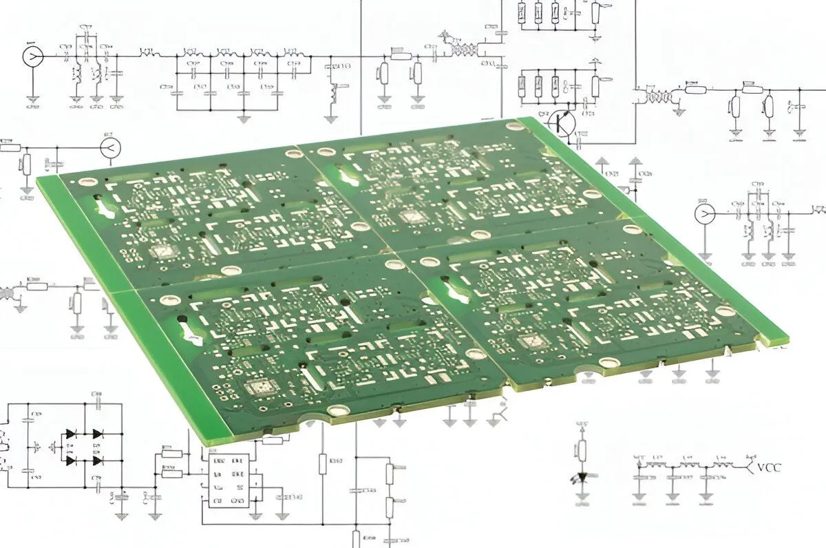
Comprehensive PCB Design & Layout Services
End‑to‑end engineering from schematic capture to final assembly files.
Multi-Layer Layout
2–20+ layers, analog, digital, mixed‑signal with proper PDN & return paths. Prepared seamlessly for fabrication.
- Length matching & diff‑pair tuning
- Impedance controlled routing
- Thermal relief & copper balance
High‑Speed Design
DDRx, PCIe, Ethernet, HDMI, MIPI with rigorous constraints and exact timing closure analysis.
- Skew budgeting & xTalk control
- Via strategy & back‑drilling
- Stack‑up co‑design with fab
RF & Microwave
50/75Ω lines, microstrip/stripline, controlled transitions & specialized grounding techniques.
- EMI/EMC best practices
- Shielding & keep‑out strategy
- Connector launch tuning
Flex / Rigid‑Flex
Precise bend radius rules, stiffener planning, and dynamic‑flex reliability for modern electronics.
- Coverlay openings & teardrops
- Hatched copper & strain relief
- ZIF/connector footprints
DFM/DFT Review
Fabrication constraints, checking for SMT assembly, test‑point planning & panelization arrays.
- Solderability & tombstoning checks
- Pick‑and‑place verification
- AOI/ICT readiness
Deliverables
Complete outputs for seamless handoff to PCB fabrication and component assembly lines.
- Gerber/ODB++, drill, fab notes
- BOM with MPN & alternates
- Pick‑and‑place, centroid, PDFs
Advanced PCB Engineering Capabilities
We engineer for signal integrity, power integrity, and long-term reliability.
- Up to 24 layers, blind/buried vias, via‑in‑pad, microvias (HDI)
- Impedance control & stack‑up co‑design with fabricator
- PDN design with stitching vias & robust decoupling strategy
- Thermal analysis & automated copper balancing
- Compliance oriented (IPC‑2221/7351, RoHS/REACH standards)
- Centralized libraries with 3D models & strict courtyard checks
Our PCB Layout Process
Transparent steps from initial requirement gathering to final release.
1. Requirement & NDA
Share schematics, constraints, preferred stack‑up, part libraries, and timelines. We always sign an NDA for IP protection.
2. Feasibility & Quote
We assess routing complexity, propose clear milestones, and share a fixed quote or hourly estimate.
3. Layout Execution
Constraint‑driven routing with periodic 3D design reviews, placement approvals, and build‑ready checks.
4. Release & Support
Deliverables: Gerber/ODB++, drill, fab notes, panel, BOM, CPL. Free support until the first prototype spin.
What We Need for Quoting
- Schematics (PDF/Source) and block diagram
- Target board size, layers, interfaces, key ICs
- Speed classes (e.g., DDR3/4, PCIe Gen, USB 3.x)
- Specials: impedance, RF, flex, via‑in‑pad, microvia
- Any preferred standards, fab/assembly house
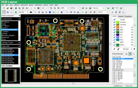
PCB Design Portfolio
Representative 3D renders and routing layouts of our recent work.

Frequently Asked Questions
Answers to common queries regarding our PCB engineering services.
Ready to start your PCB design?
Share your schematics and mechanical constraints—we’ll revert with a thorough plan and accurate quote.